Tessent Multi-die software program resolution may also help simplify essential design-for-test (DFT) duties for advanced built-in circuits (ICs) primarily based on 2.5D and 3D architectures.
The hunt for growing compact and energy-efficient units has led designers to create extra power-efficient and power-dense ICs. These next-generation units are made attainable by using 2.5D and 3D architectures that join dies vertically (3D IC) or side-by-side (2.5D) in order that they behave as a single system. To simplify the method, Siemens Digital Industries Software program has launched a brand new software program resolution referred to as Tessent Multi-die software program resolution.
The fast adoption and deployment of designs that includes densely packed dies in 2.5D and 3D units have elevated the IC take a look at complexity. To sort out this drawback the Tessent Multi-die software program resolution can generate die-to-die interconnect patterns and allow package-level exams utilizing the Boundary Scan Description Language (BS DL). The brand new software program can seamlessly work with different software program instruments utilizing an built-in Tessent platform, thus decreasing take a look at time as much as 4X.
In accordance with the corporate, the Tessent Multi-die software program is among the most complete DFT automation options for extremely advanced DFT duties related to 2.5D and 3D IC designs. The software program can be utilized with different software program from the Tessent collection corresponding to Tessent TestKompress Streaming Scan Community software program and Tessent IJTAG software program, which optimize DFT take a look at assets for every block with out concern for impacts to the remainder of the design, thereby streamlining DFT planning and implementation for the two.5D and 3D IC period. This software program permits designers to quickly generate IEEE 1838-compliant {hardware} that includes 2.5D and 3D IC architectures.
“As the boundaries of conventional 2D IC design approaches grow to be more and more clear over time, extra design groups are leveraging the ability, efficiency and type issue benefits that 2.5D and 3D IC architectures can ship. However deploying these superior schemes in new design begins with out first establishing a DFT technique that acknowledges the inherent challenges these architectures current can elevate prices and undermine aggressive timelines,” stated Laurie Balch, president and analysis director for Pedestal Analysis. “Nevertheless, by evolving DFT know-how to maintain tempo with the fast adoption of multi-dimensional designs, EDA distributors can play a key function in additional enabling world, mainstream adoption of two.5D and 3D architectures.”
Key options
• Dramatically speeds and simplifies essential DFT planning and implementation duties for next-generation ICs primarily based on 2.5D and 3D architectures
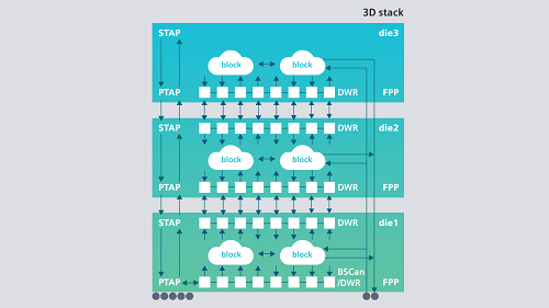
• Permits the fast technology of IEEE 1838 compliant {hardware} for 3D IC architectures
• Extracts a single Boundary Scan Description Language (BSDL) for bundle degree and generates patterns
• Extracts die-to-die BSDL and generates boundary-scan-based inter-die patterns
• Helps IEEE 1838 versatile parallel port (FPP) by leveraging the packetized information supply capabilities of the Tessent Streaming Scan Community (SSN) , which optimize DFT take a look at assets for every block with out concern for impacts to the remainder of the design
• Capability to stick and help a number of completely different requirements like IEEE 1687 and IEEE 1149.1
• Seamless integration with different Tessent merchandise utilizing an built-in Tessent platform
