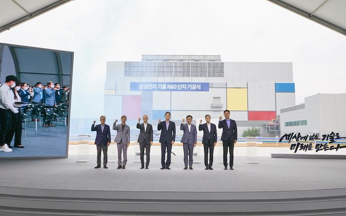
Samsung on Friday broke floor for a brand new semiconductor analysis and improvement complicated which can design new fabrication processes for reminiscence and logic, in addition to conduct basic analysis of next-generation applied sciences and supplies. The corporate plans to speculate KRW 20 trillion ($15 billion) within the new R&D facility by 2028.
To make extra aggressive logic and reminiscence chips, firms like Samsung must innovate throughout many instructions, which incorporates new supplies (for fins, for gates, for contacts, for dielectrics, simply to call just a few), transistor structure, manufacturing applied sciences, and design of precise units. In lots of circumstances, firms bodily separate basic analysis and improvement of precise course of applied sciences, however the brand new R&D middle will conduct operations throughout just about all fronts besides gadget design.
The brand new facility will deal with superior analysis on next-generation transistors and fabrication processes for reminiscence and logic chips in addition to search for brand spanking new applied sciences to ‘overcome the boundaries of semiconductor scaling.’ Basically, this implies researching new supplies and manufacturing methods in addition to creating precise manufacturing nodes. Given that each one of those R&D operations require massive scale these days, it’s not notably shocking that it’s going to require Samsung to speculate $15 billion within the middle over the subsequent six years.
Spreading basic analysis and utilized improvement operations throughout totally different places helps with bringing new expertise onboard (e.g., folks with academia background could also be unwilling to relocate too far-off from their present houses), but in addition creates discrepancy inside one firm as suggestions from totally different departments will get slower. Ideally, scientists doing pathfinding and analysis, builders designing new manufacturing nodes, fab engineers, and gadget builders ought to work collectively on a website and get suggestions from one another. However whereas Samsung’s new R&D hub will not be meant for this, it should nonetheless deliver scientists and node builders collectively, which is an enormous deal.
The brand new R&D middle might be situated at Samsung’s campus close to Giheung, South Korea, and might be occupy round 109,000 m2 (~20 soccer fields). To place the quantity right into a extra related context, Apple’s company headquarters — Apple Park — occupies round 259,000 m2 and homes over 12,000 of workers that do all the pieces from administration to analysis to product improvement.
The brand new R&D facility will work in live performance with Samsung’s current R&D line in Hwaseong (which works on reminiscence, system LSI, and foundry applied sciences) and the corporate’s manufacturing complicated in Pyeongtaek that may produce each DRAM (utilizing 10nm-class applied sciences) and logic chips (utilizing 5nm-class and thinner nodes). It’ll even be Samsung’s 12th semiconductor R&D middle. In the meantime, this would be the firm’s first semiconductor R&D facility of this scale.
Three years in the past Samsung introduced plans to spend KRW 133 trillion ($100 billion in the present day, $115 billion in 2019) on semiconductor R&D by 2030. The corporate allotted KRW 73 trillion ($54.6 billion) on R&D operations in South Korea, so investing $15 billion in a single analysis and improvement facility aligns completely with this plan.
“Our new state-of-the-art R&D complicated will change into a hub for innovation the place the very best analysis expertise from around the globe can come and develop collectively,” mentioned President Kye Hyun Kyung, who additionally heads the Machine Options (DS) Division. “We anticipate this new starting will lay the inspiration for sustainable development of our semiconductor enterprise.”
Supply: Samsung
