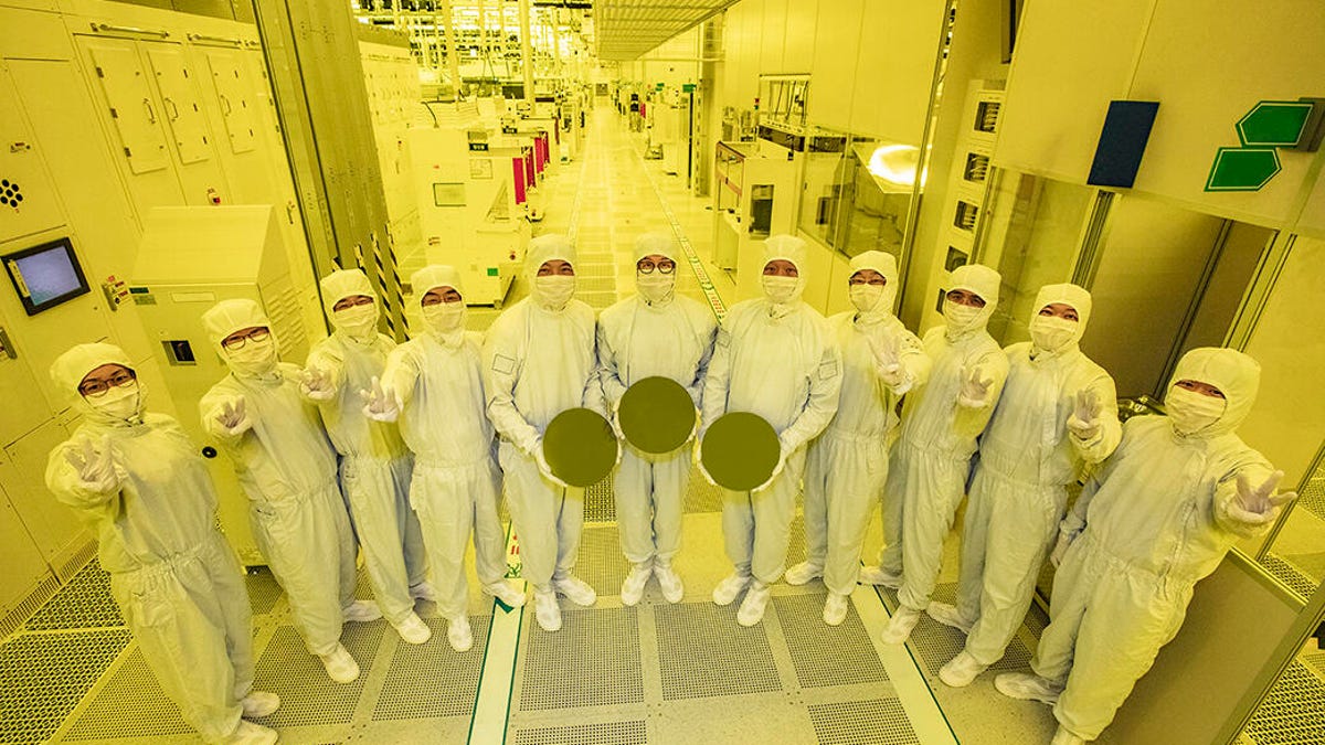
Samsung stated on Thursday that it has began mass manufacturing of chips utilizing its 3-nanometer (nm) course of node, its most superior know-how but for contract chip manufacturing.
The South Korean tech big stated its 3nm course of, in comparison with its 5nm course of, decreased energy utilization by 45% and improved efficiency by 23% with floor space decreased by 16%.
Samsung’s 3nm course of node makes use of its gate-all-around (GAA) transistor structure, referred to as Multi-Bridge-Channel FET (MBCFET) by the corporate, which packs wider channels in gates for electrical energy to circulation threw whereas lowering the voltage stage in comparison with the earlier FinFET transistor structure.
The channels are utterly surrounded by the gates, because the title GAA implies, and using all 4 sides of the channels permits extra drive present to go by way of the gates in comparison with FinFET, which solely makes use of three sides.
The South Korean tech big additionally touted that its 3nm course of node supplied a versatile design that allowed it to regulate the channel width to finest meet prospects’ wants. A follow-up second-generation 3nm course of node was additionally within the works with improved energy utilization, efficiency and floor space, Samsung stated.
Chips at the moment being made by way of its first 3nm course of node had been for a high-performance, low-power computing software, Samsung stated, whereas it plans to develop making use of the node to cellular processors. The South Korean tech big did not point out which buyer it was at the moment mass-producing the 3nm chips for.
Samsung is the world’s largest reminiscence chip maker and the second-largest contract chipmaker, or foundry. It’s competing with the world’s largest foundry Taiwan Semiconductor Manufacturing Firm (TSMC), which is gearing as much as begin mass manufacturing utilizing its personal 3nm course of node, to commercialize extra superior course of nodes first.
The important thing to the pair’s newest 3nm competitors will likely be successful extra orders over one other from giant prospects reminiscent of Qualcomm for cellular processors headed for subsequent yr’s flagship smartphones.
Final month, Samsung introduced that it plans to spend $355 billion over the subsequent 5 years on what it calls strategic companies, which embody semiconductors. Final yr, the corporate introduced that it’ll spend $17 billion to construct a brand new chip plant in Taylor, Texas.
