A high-accuracy weighing scale that may compensate for errors as a result of adjustments in temperature.
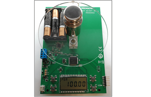
This reference design from Microchip is of a modular weighing scale that makes use of an automated calibration course of and strategies to reduce energy consumption. The weighing scale contains a digital show and a load cell to precisely measure the burden. The reference design is compact and has a low weight. The vary and precision of the dimensions are user-defined and rely on the elements chosen whereas designing. The principle benefit of this design
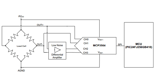
The reference design relies on the MCP3564 ADC, for enhancing the accuracy a temperature sensor may be added to the design. The design can exactly measure weight with a deviation of +/- 0.02g. The reference design presents a excessive achieve and over-sampling ratio (OSR), furthermore, the precision and accuracy of the design may be enhanced through the use of the exterior low-noise differential amplifier.
The reference design employs the PIC24FJ256GB410 microcontroller. The Excessive Low Energy (XLP) characteristic of the microcontroller allows low energy consumption, moreover, the XLP utility additionally consists of an algorithm which switches the burden scale working mode from Run mode to Sleep mode and an ultra-low energy monitoring amplifier. The design can use both an exterior DC wall adapter or a Li-Ion battery as its energy supply.
The load cell is a transducer which converts an utilized mechanical drive into {an electrical} sign immediately proportional to the magnitude of the drive. The reference design employs 4 pressure gauges as a load cell to measure the burden. Two pressure gauge measure stress and the opposite two measure compression. These 4 pressure gauges correspond to 4 resistors organized in a Wheatstone Bridge kind of circuit as proven within the determine under:
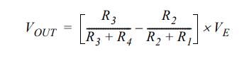
The reference design makes use of the under method to precisely measure the burden. The load cell offers a small voltage output, which is transformed to the corresponding weight by the predefined algorithm. The method used for calculating the output voltage is given under:
Options of the Reference Design:
- configurable OSR and achieve
- excessive PSRR and CMRR
- differential analog inputs (this permits direct connection of the Wheatstone Bridge)
- differential reference voltage inputs • on-chip offset and achieve calibration.
Microchip has validated this reference design and has additionally supplied all the mandatory design sources such because the BoM, Gerber file, schematics, software program information, and so on. to simplify the event of this reference design. It is advisable signal as much as entry the design information, you may get all of the design sources right here.
