Nvidia introduced new particulars about its Grace CPU Superchip prematurely of its Sizzling Chips 34 presentation subsequent week, revealing that the chips come fabbed on the 4N course of. Nvidia additionally shared extra details about the structure and information cloth, together with extra efficiency and effectivity benchmarks. Nvidia hasn’t made its official presentation at Sizzling Chips but — we’ll add the finer-grained particulars after the session — however the info shared in the present day provides us the broad strokes because the Grace chips and servers work their method to market within the first half of 2023.
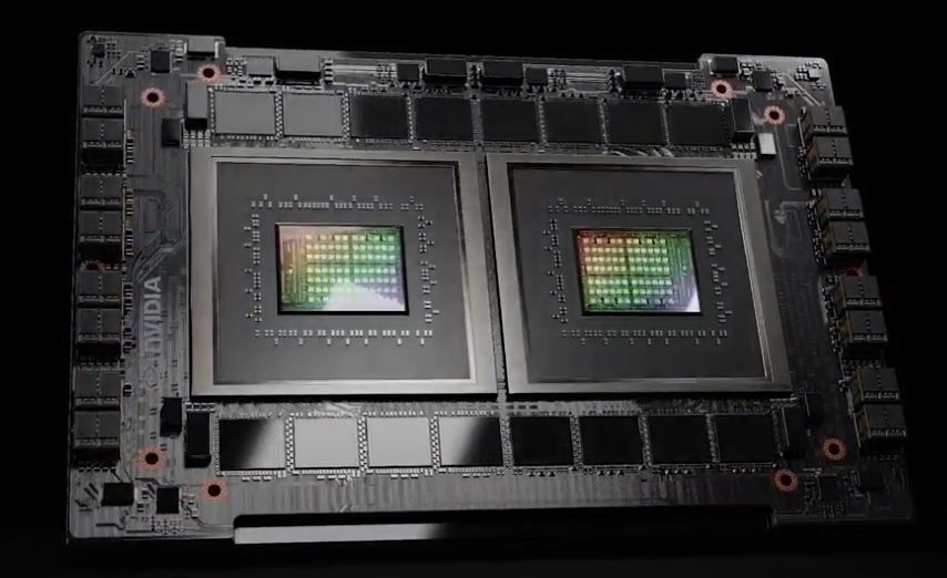
As a fast reminder, Nvidia’s Grace CPU is the corporate’s first CPU-only Arm chip designed for the information heart and comes as two chips on one motherboard, totaling 144 cores, whereas the Grace Hopper Superchip combines a Hopper GPU and the Grace CPU on the identical board.
Among the many most necessary disclosures, Nvidia lastly formally confirmed that the Grace CPUs use the TSMC 4N course of. TSMC lists the “N4” 4nm course of beneath its 5nm node household, describing it as an enhanced model of the 5nm node. Nvidia makes use of a specialised variant of this node, dubbed ‘4N,’ that’s optimized particularly for its GPUs and CPUs.
(Picture credit score: Nvidia)
These kind of specialised nodes have gotten extra widespread as Moore’s Legislation wanes and shrinking the transistors turns into more durable and costlier with every new node. To allow customized course of nodes like Nvidia’s 4N, chip designers and foundries work hand-in-hand through the use of Design-Know-how Co-Optimization (DTCO) to dial in customized energy, efficiency, and space (PPA) traits for his or her particular merchandise.
Nvidia has beforehand revealed that it makes use of off-the-shelf Arm Neoverse cores for its Grace CPUs, however the firm nonetheless hasn’t specified which particular model it makes use of. Nonetheless, Nvidia has disclosed that Grace makes use of Arm v9 cores and helps SVE2, and the Neoverse N2 platform is Arm’s first IP to help Arm v9 and extensions like SVE2. The N2 Perseus platform comes as a 5nm design (keep in mind, N4 is in TSMC’s 5nm household) and helps PCIe Gen 5.0, DDR5, HBM3, CCIX 2.0, and CXL 2.0. The Perseus design is optimized for performance-per-power (watt) and performance-per-area. Arm says that its next-gen cores, Poseidon, will not arrive in the marketplace till 2024, making these cores a much less probably candidate given Grace’s early 2023 launch date.
Nvidia Grace Hopper CPU Structure
Nvidia’s new Nvidia Scalable Coherency Cloth (SCF) is a mesh interconnect that appears similar to the usual CMN-700 Coherent Mesh Community that’s used with Arm Neoverse cores.
The Nvidia SCF gives 3.2 TB/s of bi-sectional bandwidth between the varied Grace chip models, just like the CPU cores, reminiscence, and I/O, to not point out the NVLink-C2C interface that ties the chip to the opposite unit current on the motherboard, be it one other Grace CPU or the Hopper GPU.
(Picture credit score: Nvidia )
The mesh helps 72+ cores, and every CPU has 117MB of whole L3 cache. Nvidia says the primary block diagram within the album above is a ‘potential topology for illustrative functions,’ and its alignment does not completely agree with the second diagram.
This diagram exhibits the chip with eight SCF Cache partitions (SCC) that seem like L3 cache slices (we’ll study extra particulars within the presentation) together with eight CPU models (these seem like clusters of cores). The SCC and cores are related to Cache Change Nodes (CSN) in teams of two, with the CSN then residing on the SCF mesh cloth to supply an interface between the CPU cores and reminiscence to the remainder of the chip. SCF additionally helps coherency throughout as much as 4 sockets with Coherent NVLink.
(Picture credit score: Nvidia )
Nvidia additionally shared this diagram, displaying that every Grace CPU helps as much as 68 PCIe lanes and as much as 4 PCIe 5.0 x16 connections. Every x16 connection helps as much as 128 GB/s of bidirectional throughput (the x16 hyperlinks might be bifurcated to 2 x8 hyperlinks). We additionally see 16 dual-channel LPDDR5X reminiscence controllers (MC).
Nonetheless, this diagram is completely different than the primary — it exhibits the L3 cache as two contiguous blocks related to quad-core CPU clusters, which makes way more sense than the prior diagram and totals as much as 72 cores within the chip. Nonetheless, we do not see the separate SCF partitions or the CSN nodes from the primary diagram, which lends a little bit of confusion. We’ll suss this out throughout the presentation and replace as needed.
Nvidia tells us that the Scalable Coherency Cloth (SCF) is its proprietary design, however Arm permits its companions to customise the CMN-700 mesh by adjusting core counts, cache sizes, and utilizing several types of reminiscence, reminiscent of DDR5 and HBM, and deciding on varied interfaces, like PCIe 5.0, CXL, and CCIX. Meaning it’s potential Nvidia makes use of a highly-customized CMN-700 implementation for the on-die cloth.

