The corporate behind X-NAND flash reminiscence claims to have doubled the velocity of its storage for its second technology of chips, as reported by Blocks and Information (opens in new tab), by enabling information writes in parallel. This manner, X-NAND can ship SLC ranges of efficiency from QLC flash, which is cheaper and is available in bigger capacities.
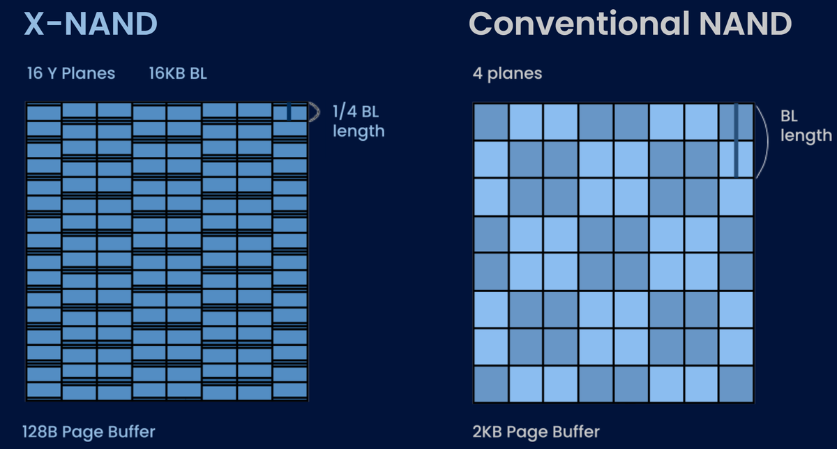
Neo Semiconductor’s X-NAND structure may be utilized to all generations of flash reminiscence and entails dividing every airplane of the 3D matrix into 4 to 16 sub-planes, every of which may be accessed in parallel, utilizing web page buffers to optimize velocity. Gen 2 X-NAND (opens in new tab) (PDF) takes this concept and compresses it down, utilizing one airplane to jot down to a different, whereas earlier than, it could have used three planes to jot down to a fourth. See our characteristic right here for a fuller write-up of how the know-how works.

