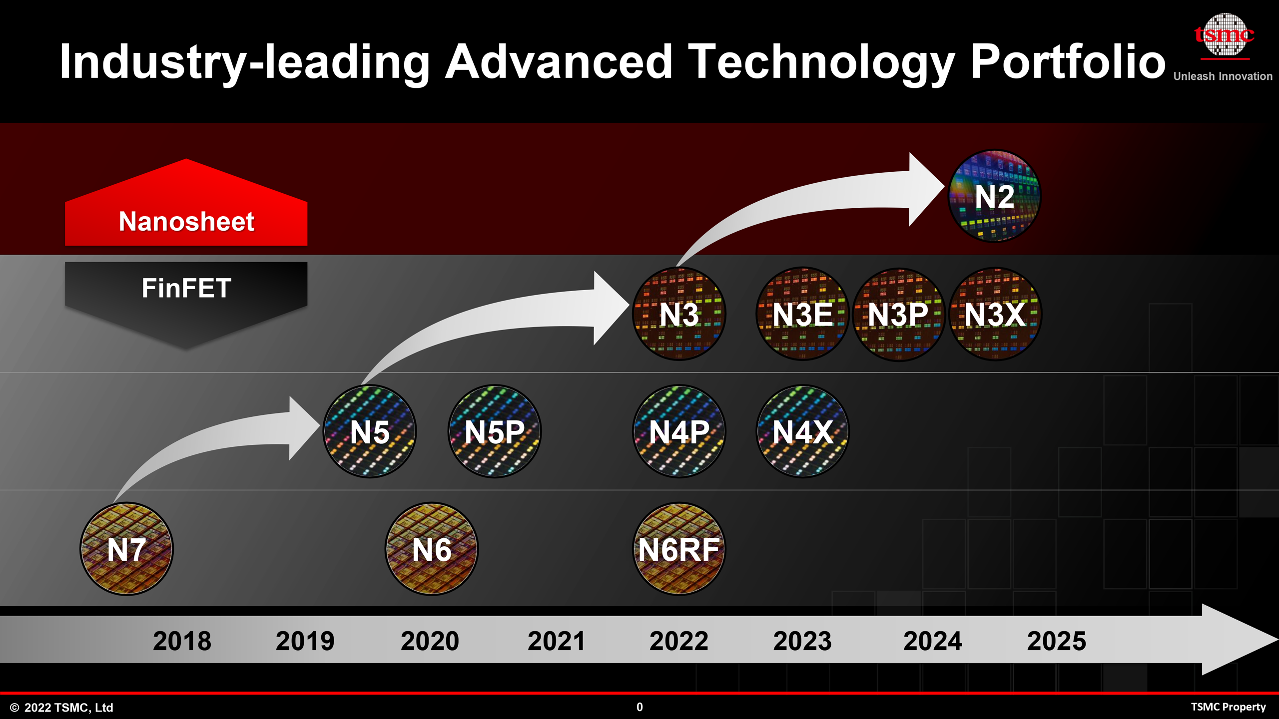
At its 2022 Expertise Symposium, TSMC formally unveiled its N2 (2 nm class) fabrication expertise, which is slated to enter manufacturing a while in 2025 and can be TSMC’s first node to make use of their nanosheet-based gate-all-around field-effect transistors (GAAFETs). The brand new node will allow chip designers to considerably cut back the facility consumption of their merchandise, however the velocity and transistor density enhancements appear significantly much less tangible.
TSMC’s N2 is a brand-new platform that extensively makes use of EUV lithography and introduces GAAFETs (which TSMC calls nanosheet transistors) in addition to bottom energy supply. The brand new gate-all-around transistor construction guarantees well-published benefits, corresponding to vastly diminished leakage present (now that the gates are round all 4 sides of the channel) in addition to capacity to regulate channel width to extend efficiency or decrease energy consumption. As for the bottom energy rail, it’s typically designed to allow higher energy supply to transistors, providing an answer to the issue of accelerating resistances within the back-end-of-line (BEOL). The brand new energy supply is slated to extend transistor efficiency and decrease energy consumption.
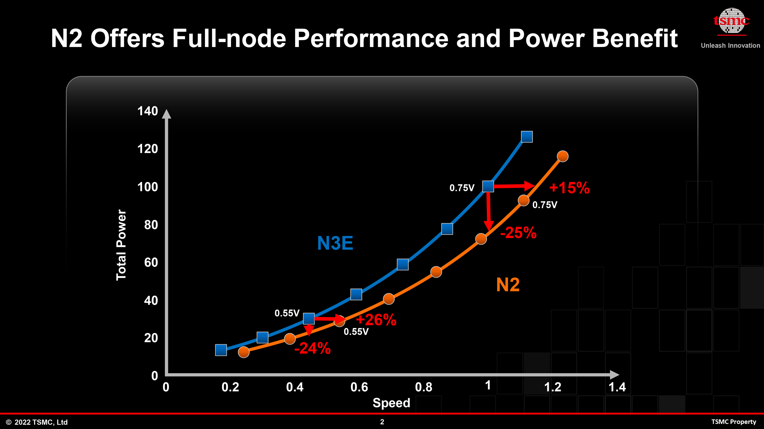
From function set standpoint, TSMC’s N2 seems to be like a really promising expertise. As for precise numbers, TSMC guarantees that N2 will permit chip designers to extend efficiency by 10% to fifteen% on the similar energy and transistor rely, or cut back energy consumption on the similar frequency and complexity by 25% ~ 30%, all of the whereas rising chip density by over 1.1-fold when in comparison with N3E node.
| Marketed PPA Enhancements of New Course of Applied sciences Information introduced throughout convention calls, occasions, press briefings and press releases |
|||||
| TSMC | |||||
| N5 vs N7 |
N3 vs N5 |
N3E vs N5 |
N2 vs N3E |
||
| Energy | -30% | -25-30% | -34% | -25-30% | |
| Efficiency | +15% | +10-15% | +18% | +10-15% | |
| Chip Density* | ? | ? | ~1.3X | >1.1X | |
| Quantity Manufacturing |
Q2 2022 | H2 2022 | Q2/Q3 2023 | H2 2025 | |
*Chip density printed by TSMC displays ‘combined’ chip density consisting of fifty% logic, 30% SRAM, and 20% analog.
Versus N3E, the efficiency enhancements and energy reductions enabled by TSMC’s N2 node are according to what the foundry’s new nodes usually usher in. However the so-called chip density enhancements (which ought to mirror transistor density beneficial properties) are just a bit over 10%, which isn’t significantly inspiring, particularly contemplating that N3E already affords a barely decrease transistor density when in comparison with vanilla N3. Maintaining in thoughts that SRAM and analog circuits barely scale nowadays, mediocre enhancements in transistor density of precise chips ought to most likely be anticipated nowadays. Nonetheless, a chip density enchancment of 10% in about three years is actually not nice information for GPUs and different chips that stay or die primarily based on quickly rising their transistor counts.
Taking into consideration that by the point TSMC’s N2 enters manufacturing the corporate can even have the density-optimized N3S node, it will seem that the foundry may have two course of applied sciences primarily based on several types of transistors but providing very related transistor densities, one thing that has by no means occurred earlier than.
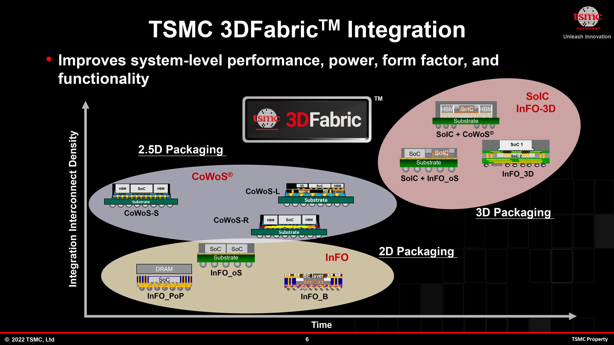
As regular, TSMC will provide their N2 node with numerous options and knobs to permit chip designers to optimize for issues like cellular and high-performance computing designs (notice that TSMC calls HPC every little thing that’s not cellular, automotive or specialty. which incorporates every little thing from a low-power laptop computer CPU to a high-end compute GPU aimed toward supercomputers). Additionally, platform choices embody one thing that TSMC calls ‘chiplet integration’, which most likely signifies that TSMC allow its clients to simply combine N2 chips into multi-chiplet packages made utilizing numerous nodes. Since transistor density scaling is slowing down and new course of applied sciences are getting costlier to make use of, multi-chiplet packages are going to change into extra widespread within the coming years as builders can be utilizing them to optimize their designs and prices.
TSMC expects to begin threat manufacturing of chips utilizing its N2 fabrication course of typically within the second half of 2024, which signifies that the expertise ought to be obtainable for top quantity manufacturing (HVM) of economic merchandise within the second half of 2025. However, contemplating the size of contemporary semiconductor manufacturing cycles, it is probably extra pragmatic to anticipate the primary N2 chips to change into obtainable both very late in 2025 or 2026, if every little thing goes as deliberate.
