When TSMC initially launched its N2 (2 nm class) course of expertise earlier this month, the corporate outlined how the brand new node could be constructed on the again of two new cutting-edge fab strategies: gate-all-around transistors, and bottom energy rails. However, as we have since discovered from final week’s EU symposium, TSMC’s plans are a bit extra nuanced than first introduced. Not like a few of their rivals, TSMC won’t be implementing each applied sciences within the preliminary model of their N2 node. As an alternative, the primary iteration of N2 will solely be implementing gate-all-around transistors, with bottom energy supply to come back with a later model of the node.
To this point, TSMC has talked about two distinctive options of N2: nano sheet gate-all-around (GAA) transistors, and bottom energy rails. GAA transistors have two distinctive benefits over FinFETs: they remedy many challenges related to the leakage present since GAAFET’s channels are horizontal and are surrounded by gates round all 4 sides. In the meantime, bottom energy rail enabled improved energy supply to transistors, which will increase efficiency and lowers energy consumption.
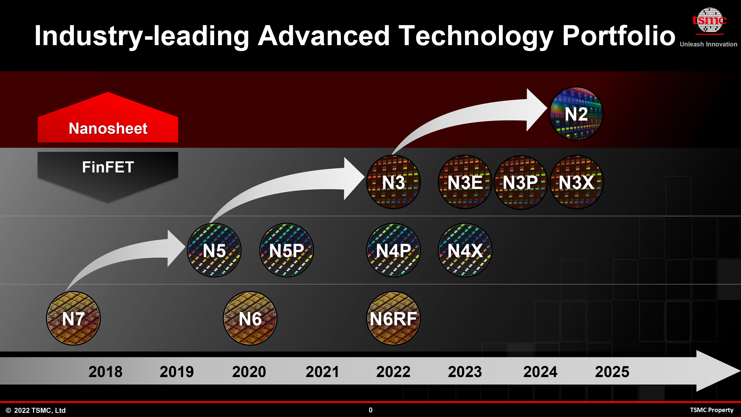
However, because it seems, TSMC shouldn’t be planning to start out with each nanosheet GAA transistors and bottom energy rails within the preliminary era of its N2 course of expertise. As disclosed by the corporate final week at their EU symposium, the primary era of N2 will solely characteristic gate-all-around transistors. Bottom energy supply, however, will come later with extra superior implementations of N2.
At this level the corporate hasn’t stated an excessive amount of as to why they are not rolling out bottom energy supply as a part of their preliminary N2 node. However, in discussing the bifurcation, TSMC has famous that bottom energy supply will finally add extra course of steps, which the corporate is seemingly seeking to keep away from on their first strive with GAAFETs.
The dearth of bottom energy supply within the authentic model of the N2 fabrication expertise maybe explains relatively reasonable efficiency enchancment of N2 when in comparison with N3E node. Whereas for high-performance computing (CPUs, accelerators, and so on.) a ten% to fifteen% efficiency enchancment on the identical energy and complexity doesn’t appear to be spectacular, a 25% to 30% energy drop on the identical velocity and complexity appears to be superb for cellular purposes.
| Marketed PPA Enhancements of New Course of Applied sciences Information introduced throughout convention calls, occasions, press briefings and press releases |
|||||
| TSMC | |||||
| N5 vs N7 |
N3 vs N5 |
N3E vs N5 |
N2 vs N3E |
||
| Energy | -30% | -25-30% | -34% | -25-30% | |
| Efficiency | +15% | +10-15% | +18% | +10-15% | |
| Chip Density* | ? | ? | ~1.3X | >1.1X | |
| Quantity Manufacturing |
Q2 2022 | H2 2022 | Q2/Q3 2023 | H2 2025 | |
*Chip density revealed by TSMC displays ‘blended’ chip density consisting of fifty% logic, 30% SRAM, and 20% analog.
Contemplating that TSMC all the time provides a number of variations of its nodes, that TSMC has a number of variants deliberate for N2 shouldn’t be all that shocking. Nonetheless, it’s a bit odd to see that TSMC is taking a relatively lengthy highway to bottom energy supply.
In contrast and contrasted to the competitors, this can find yourself being a notable distinction from how rival Intel is planning to deal with their very own GAAFET/bottom energy transition with the Intel 20A course of. Intel intends to introduce its GAA RibbonFET transistors and PowerVia interconnects collectively in mid-2024 – going as far as to create an inner pseudo node simply to concentrate on RibbonFET growth. TSMC, however, is taking a extra cautious strategy to dangers and improvements, one which probably has TSMC shifting at a slower tempo, however can be an strategy that has historically been a greater match for TSMC’s have to ship extra fixed and constant updates to its fab choices.
And whereas we’re nonetheless a number of years out, will probably be attention-grabbing to see what this implies for the competitiveness of TSMC’s first-generation N2 node. Will a GAAFET course of with out bottom energy supply be at a significant drawback? Per present schedules, we’ll discover out the reply to that within the second half of 2025, when TSMC’s first N2 node is slated to enter high-volume manufacturing (HVM).
