
What seems to be an inner TSMC slide charting the event progress of the N3E course of has been shared by tech fanatic HS Kuo (opens in new tab) on Twitter. Not too long ago, we heard from Taiwan’s enterprise media that N3 was going to hit mass manufacturing come September, however we haven’t had a lot details about the progress of N3E since again in March.
To rapidly recap, TSMC N3E is an ‘Enhanced’ model of the N3 course of, which was initially scheduled (opens in new tab) (PDF) for mass manufacturing a yr after N3. Nevertheless, the brand new however undated slide (please add a pinch of salt) from Mr. Kuo signifies that the event of N3E is progressing properly and is even “forward of plan.”
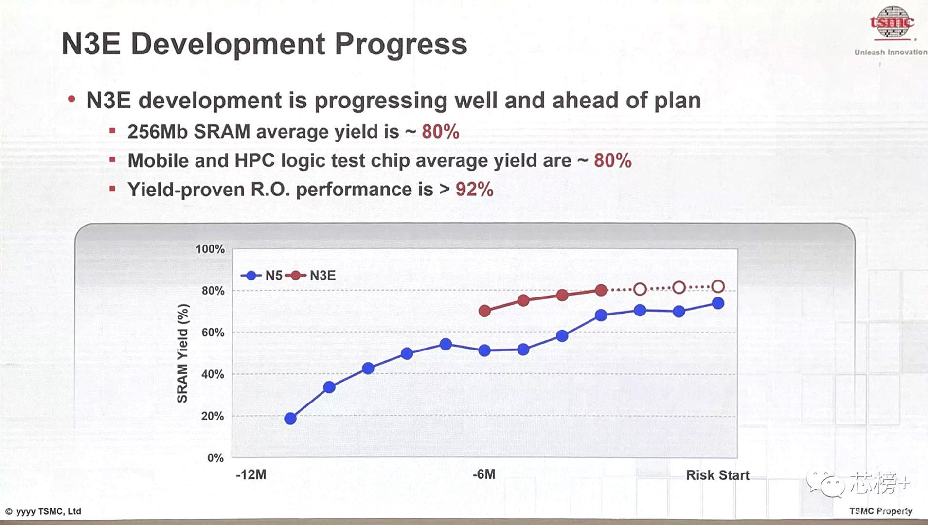
The chart suggests N3E SRAM yields are monitoring considerably above N3, beginning about six months forward of danger manufacturing. Presently, the typical 256Mb SRAM yield is about 80%, it’s claimed. Additionally spectacular is that Cell and HPC check chips yield about 80%. Lastly, yield-proven ring oscillator efficiency is healthier than 92%.
We aren’t stunned by earlier experiences into N3E that it’s progressing so properly. TSMC designed N3E with an improved course of window, with barely decrease transistor density, which naturally comes with the advantage of higher yields. Different touted advantages of N3E are higher clock speeds and decrease energy utilization.
