
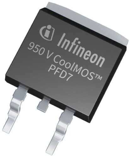
To handle modern market wants for improved type components and energy-efficient merchandise, Infineon Applied sciences has developed a brand new CoolMOS PFD7 high-voltage MOSFET household, setting a brand new benchmark in 950 V superjunction (SJ) expertise. The brand new 950 V sequence combines excellent efficiency with state-of-the-art ease of use and options an built-in quick physique diode making certain a strong system and in flip lowered bill-of-material (BOM). Tailor-made to ultrahigh-power density in addition to the very best effectivity designs, the brand new merchandise are primarily addressing lighting programs, in addition to client and industrial SMPS purposes.
The brand new merchandise are appropriate for flyback, PFC, and LLC/LCC designs, together with half- or full-bridge configurations making commutation strong and dependable. By integrating an ultra-fast physique diode with ultra-low reverse restoration cost (Q rr), they provide onerous commutation ruggedness and reliability. This makes it essentially the most strong SJ MOSFET on this voltage class, enabling utilization throughout all topologies within the focused purposes. As well as, considerably lowered switching losses (E OSS, Q OSS, and Q g) enhance effectivity in hard- and soft-switching purposes and end in as much as 4°Ok decrease MOSFET temperature in comparison with 900 V CoolMOS C3 SJ MOSFET. The brand new merchandise enhance light- and full-load PFC effectivity by greater than 0.2 p.c whereas matching the efficiency close to LLC effectivity, contributing to a greener world.
The brand new household affords as much as 55 p.c decrease on resistance (R DS(on)) gadgets in numerous SMD and THD packages, like 450 mΩ in DPAK or 60 mΩ in TO247. This permits designers to make use of smaller packages and increase energy density and board house financial savings at lowered BOM and manufacturing prices. A gate-source threshold voltage (V (GS),th) of three V and smallest V (GS),th variation of ±0.5 V, makes the brand new gadgets straightforward to design-in and drive, resulting in elevated design freedom. Because of the low threshold voltage and tolerance, MOSFET linear mode operation is prevented whereas permitting decrease driving voltage and lowered idle loss. Moreover, a 60 p.c improved gate cost in comparison with CoolMOS C3 leads to considerably lowered driving losses. ESD ruggedness is ensured with a human physique mannequin (HBM) stage of sophistication 2, offering lowered ESD-related failures and improved manufacturing yield.
