One pattern within the excessive efficiency computing (HPC) area that’s changing into more and more clear is that energy consumption per chip and per rack unit shouldn’t be going to cease with the bounds of air cooling. As supercomputers and different excessive efficiency methods have already hit – and in some instances exceeded these limits – energy necessities and energy densities have continued to scale up. And primarily based on the information from TSMC’s current annual expertise symposium, we must always anticipate to see this pattern proceed as TSMC lays the groundwork for even denser chip configurations.
The issue at hand shouldn’t be a brand new one: transistor energy consumption is not cutting down almost as rapidly as transistor sizes. And as chipmakers aren’t about to depart efficiency on the desk (and fail to ship semi-annual will increase for his or her clients), within the HPC area energy per transistor is rapidly rising. As an extra wrinkle, chiplets are paving the way in which in the direction of developing chips with much more silicon than conventional reticle limits, which is nice for efficiency and latency, however much more problematic for cooling.
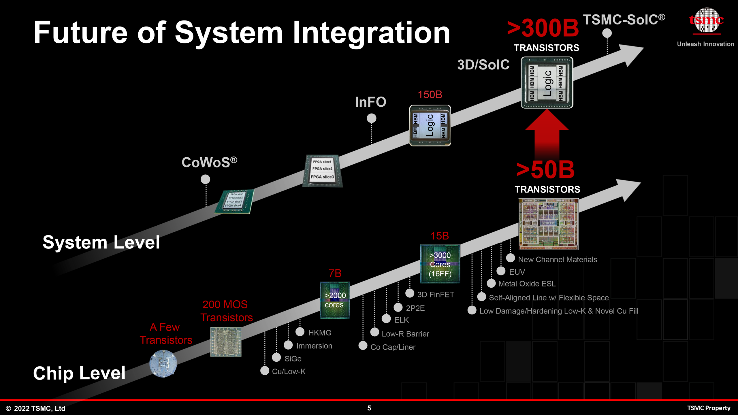
Enabling this sort of silicon and energy development has been fashionable applied sciences like TSMC’a CoWoS and InFO, which permit chipmakers to construct built-in multi-chiplet system-in-packages (SiPs) with as a lot a double the quantity of silicon in any other case allowed by TSMC’s reticle limits. By 2024, developments of TSMC’s CoWoS packaging expertise will allow constructing even bigger multi-chiplet SiP, with TSMC anticipating stitching collectively upwards of 4 reticle-sized chiplets, This can allow large ranges of complexity (over 300 billion transistor per SiP is a risk that TSMC and its companions are ) and efficiency, however naturally at the price of formidable energy consumption and warmth technology.
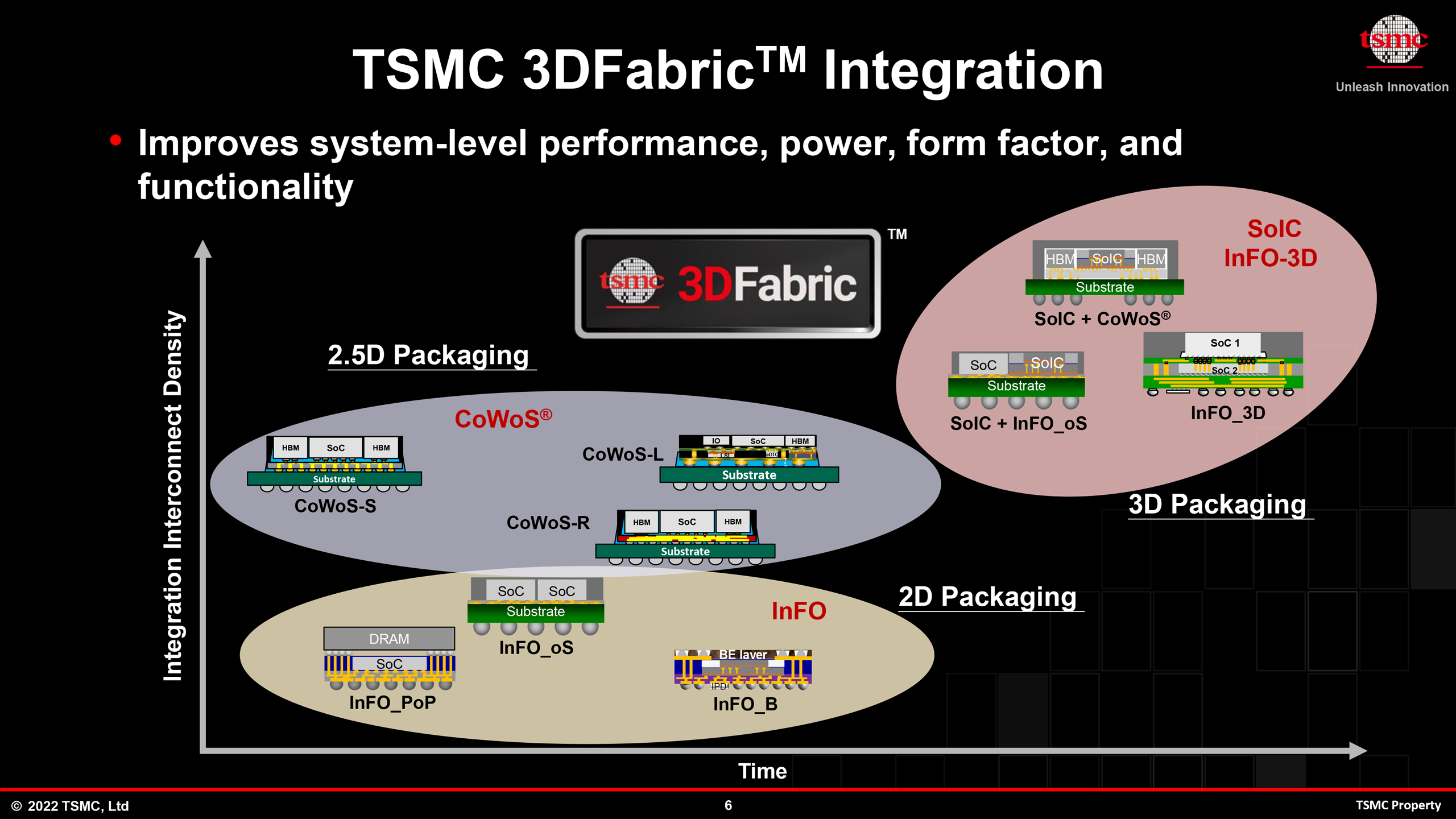
Already, flagship merchandise like NVIDIA’s H100 accelerator module require upwards of 700W of energy for peak efficiency. So the prospect of a number of, GH100-sized chiplets on a single product is elevating eyebrows – and energy budgets. TSMC envisions that a number of years down the street there shall be multi-chiplet SiPs with an influence consumption of round 1000W and even greater, Making a cooling problem.
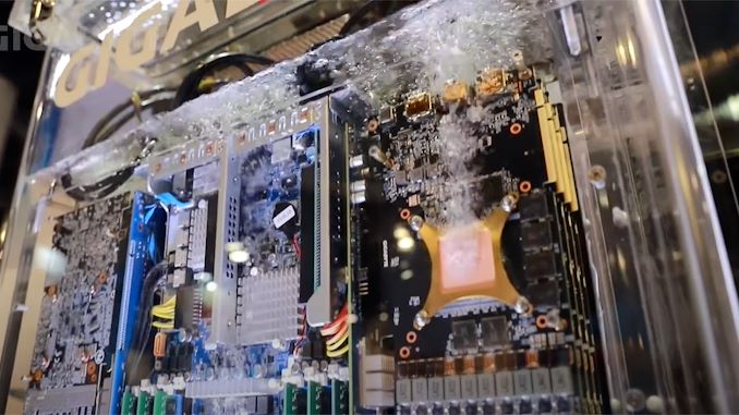
At 700W, H100 already requires liquid cooling; and the story is way the identical for the chiplet primarily based Ponte Vecchio from Intel, and AMD’s Intuition MI250X. However even conventional liquid cooling has its limits. By the point chips attain a cumulative 1 kW, TSMC envisions that datacenters might want to use immersion liquid cooling methods for such excessive AI and HPC processors. Immersion liquid cooling, in flip, would require rearchitecting datacenters themselves, which shall be a serious change in design and a serious problem in continuity.
The short-tem challenges apart, as soon as datacenters are setup for immersion liquid cooling, they are going to be prepared for even hotter chips. Liquid immersion cooling has a number of potential for dealing with massive cooling masses, which is one cause why Intel is investing closely on this expertise in an try and make it extra mainstream.
Along with immersion liquid cooling, there’s one other expertise that can be utilized to chill down ultra-hot chips — on-chip water cooling. Final yr TSMC revealed that it had experimented with on-chip water cooling and mentioned that even 2.6 kW SiPs could possibly be cooled down utilizing this expertise. However after all, on-chip water cooling is a particularly costly expertise by itself, which can drive prices of these excessive AI and HPC options to unprecedented ranges.
None the much less, whereas the long run is not set in stone, seemingly it has been forged in silicon. TSMC’s chipmaking purchasers have clients prepared to pay a high greenback for these ultra-high-performance options (assume operators of hyperscale cloud datacenters), even with the excessive prices and technical complexity that entails. Which to carry issues again to the place we began, is why TSMC has been creating CoWoS and InFO packaging processes on the primary place – as a result of there are clients prepared and keen to interrupt the reticle restrict by way of chiplet expertise. We’re already seeing a few of this at the moment with merchandise like Cerebras’ huge Wafer Scale Engine processor, and by way of massive chiplets, TSMC is getting ready to make smaller (however nonetheless reticle-breaking) designs extra accessible to their wider buyer base.
Such excessive necessities for efficiency, packaging, and cooling not solely push producers of semiconductors, servers, and cooling methods to their limits, but in addition require modifications of cloud datacenters. If certainly huge SiPs for AI and HPC workloads change into widespread, cloud datacenters shall be fully totally different within the coming years.
