Alongside their Zen CPU structure and RDNA shopper GPU structure updates, AMD this afternoon can also be updating their roadmap for his or her CDNA server GPU structure and associated Intuition merchandise. And whereas CPUs and shopper GPUs are arguably on a relatively simple path for the subsequent two years, AMD intends to shake up its server GPU choices in a giant approach.
Let’s begin first with AMD’s server GPU architectural roadmap. Following AMD’s present CDNA 2 structure, which is getting used within the MI200 sequence Intuition Accelerators, can be CDNA 3. And in contrast to AMD’s different roadmaps, the corporate isn’t providing a two-year view right here. As a substitute, the server GPU roadmap solely goes out one 12 months – to 2023 – with AMD’s subsequent server GPU structure set to launch subsequent 12 months.
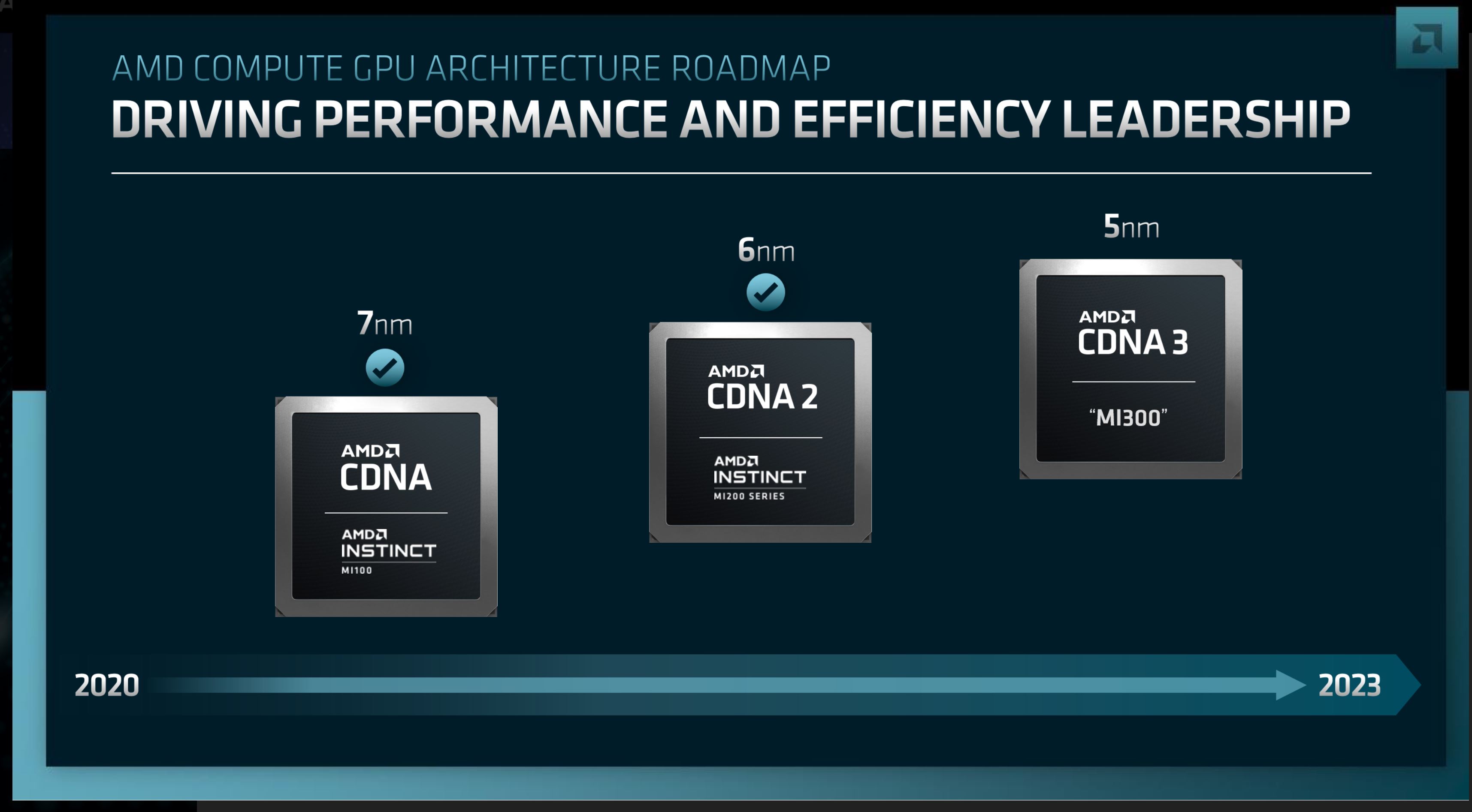
Our first take a look at CDNA 3 comes with fairly a little bit of element. With a 2023 launch AMD isn’t holding again on info fairly as a lot as they do elsewhere. Consequently, they’re divulging info on every little thing from the structure to some fundamental details about one of many merchandise CDNA 3 will go in to – an information middle APU fabricated from CPU and GPU chiplets.
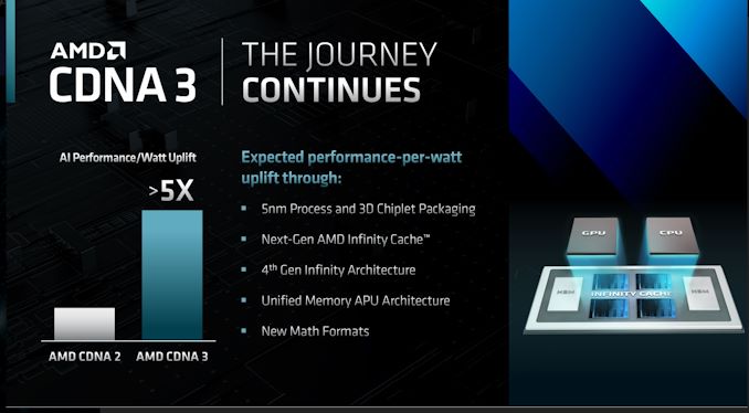
Taking issues from the highest, GPUs primarily based on the CDNA 3 structure can be constructed on a 5nm course of. And just like the CDNA 2-based MI200 accelerators earlier than it, will depend on a chiplets to mix reminiscence, cache, and processor cores all on a single bundle. Notably, AMD is looking this a “3D chiplet” design, which suggests that not solely are chiplets being stacked on to a substrate, however that some form of chip goes to be stacked on prime of different chiplets as effectively, ala AMD’s V-Cache for Zen 3 CPUs.
That comparability is especially apt right here as AMD goes to be introducing its Infinity Cache know-how into the CDNA 3 structure. And, just like the V-Cache instance above, judging from AMD’s paintings it seems that they will be stacking the cache with the logic as separate dies, relatively than integrating it right into a monolithic die like their shopper GPUs. Due to this stacked nature, the Infinity Cache chiplets for CDNA 3 will go beneath the processor chiplets, which AMD seemingly placing the very, very power-hungry logic chiplets on the prime of the stack with the intention to successfully cool them.
CDNA 3 may even be using AMD’s 4th era Infinity Structure. We’ll have extra about that in a separate article, however the quick model is that for GPUs, IA4 goes hand-in-hand with AMD’s chiplet improvements. Particularly, it should allow 2.5D/3D stacked chips for use with IA, permitting for the entire chips inside a bundle to share a unified and absolutely coherent reminiscence subsystem. This can be a large leap past IA3 and the present MI200 accelerators, which though providing reminiscence coherency, doesn’t have a unified reminiscence deal with area. So whereas MI200 accelerators operate as basically two GPUs on a single bundle, IA4 will let CDNA 3/MI300 accelerators to behave as a single chip, regardless of the disaggregated nature of the chiplets.
AMD’s diagrams additionally present HBM reminiscence being as soon as once more used right here. AMD doesn’t specify what model of HBM, however given the 2023 timeframe it’s a really secure guess that it is going to be HBM3.
Architecturally, AMD may even be taking a number of steps to enhance the AI efficiency of their high-performance accelerator. Based on the corporate they’re including assist for brand spanking new combined precision math codecs. And whereas it’s not being explicitly acknowledged at this time, AMD’s >5x enchancment in performance-per-watt in AI workloads strongly implies that AMD is considerably transforming and increasing their matrix cores for CNDA 3, as 5x is effectively in extra of what fab enhancements alone can ship.
MI300: AMD’s First Disaggregated Information Middle APU
However AMD isn’t stopping by simply constructing an even bigger GPU, nor are they unifying the reminiscence pool for a multi-chiplet structure merely to have GPUs figuring out of a shared reminiscence pool. As a substitute, AMD’s ambitions are a lot higher than that. With high-performance CPU and GPU cores at their disposal, AMD is taking the subsequent step in integration and is constructing a disaggregated, information middle APU – a chip that mixes CPU and GPU cores on to a single bundle.

The information middle APU, which is at present codenamed MI300, is one thing AMD has been constructing to for some time now. With MI200 and Infinity Structure 3 permitting AMD CPUs and GPUs to work along with a coherent reminiscence structure, the subsequent step for some time has been to convey the CPU and GPU additional collectively, each when it comes to packaging and reminiscence structure.
For reminiscence issues particularly, a unified structure brings MI300 a pair main advantages. From a efficiency standpoint, this improves issues by eliminating redundant reminiscence copies; processors not want to repeat information over to their very own devoted reminiscence pool to entry/alter that information. The unified reminiscence pool additionally signifies that there isn’t a second pool of reminiscence chips required – on this case, the DRAM that may usually be hooked up to the CPU.
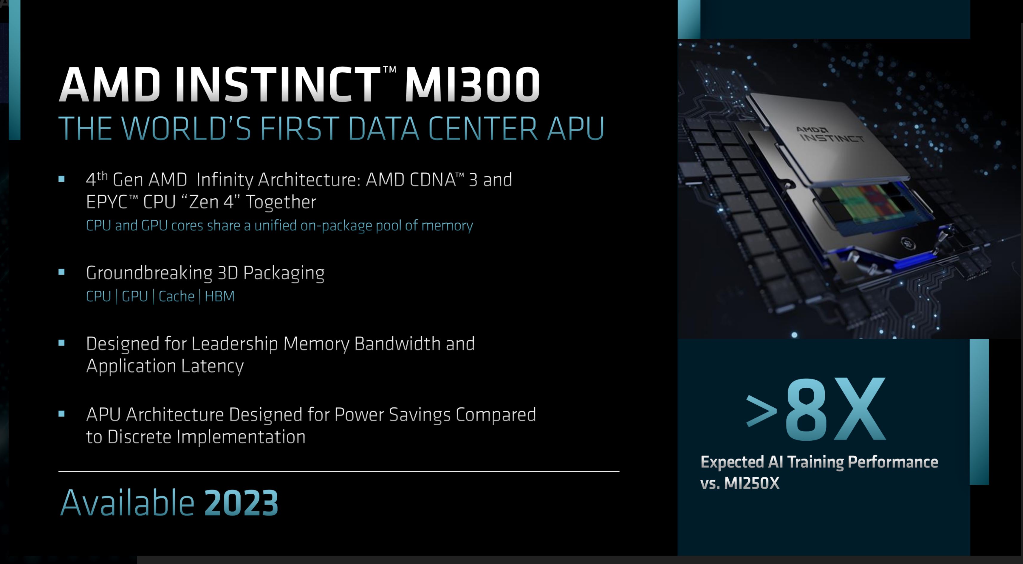
MI300 will mix CDNA 3 GPU chiplets and Zen 4 CPU chiplets on to a single processor bundle. Each of those processor swimming pools, in flip, will share the on-package HBM reminiscence. And, presumably, the Infinity Cache as effectively.
As beforehand talked about, AMD goes to be closely leveraging chiplets with the intention to accomplish this. The CPU cores, GPU cores, Infinity Cache, and HBM are all completely different chiplets, a few of which can be stacked upon one another. So this can be chip in contrast to the rest AMD has constructed earlier than, and it is going to be essentially the most concerned effort but from AMD to combine chiplets into their product designs.
In the meantime, AMD is being very express about the truth that they’re gunning for market management when it comes to reminiscence bandwidth and software latency. Which if AMD can pull it off, can be a major accomplishment for the corporate. With that mentioned, they aren’t the primary firm to pair HBM with CPU cores – Intel’s Sapphire Rapids Xeon CPU will declare that accomplishment – so it is going to be fascinating to see simply how MI300 pans out in that regard.
As for the extra particular matter of AI efficiency, AMD is claiming that the APU will supply higher than 8x the coaching efficiency of the MI250X accelerator. Which is additional proof that AMD goes to be making some large enhancements to their GPU matrix cores versus the MI200 sequence.
Total, AMD’s server GPU trajectory is pretty just like what we’ve seen Intel and NVIDIA announce prior to now a number of months. All three corporations are constructing in the direction of mixed CPU+GPU merchandise; NVIDIA with Grace Hopper (Grace + H100), Intel with Falcon Shores XPUs (combine & match CPU + GPU), and now MI300 with its use of each CPU and GPU chiplets on a single bundle. In all three circumstances, these applied sciences are aimed toward combining the perfect of CPUs with the perfect of GPUs for workloads that aren’t purely certain by both – and in AMD’s case, the corporate believes they’ve the perfect CPUs and the perfect GPUs going into this course of.
Anticipate to see much more on CDNA 3 and MI300 over the approaching months.
