
Or to place it in Micron’s personal phrases, this can be a “watershed second for storage innovation,” serving as the primary proof that it could possibly scale 3D NAND flash to greater than 200 layers in quantity manufacturing. Not that it was a straightforward achievement by any stretch, however an essential one.
“This groundbreaking know-how required intensive innovation, together with superior course of capabilities to create excessive facet ratio constructions, novel supplies developments and modern design enhancements that construct on our market-leading 176-layer NAND know-how,” stated Scott DeBoer, government vp of know-how and merchandise at Micron.

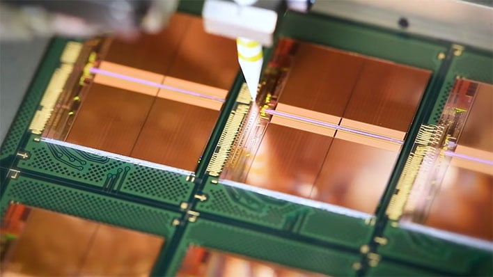
It is an oversimplified analogy, however Micron’s 3D NAND takes the identical basic strategy. In accordance with Micron, its 232-layer answer allows the trade quickest NAND I/O pace at 2.4GB/s, which is 50 p.c sooner than the earlier technology 176-layer answer. It additionally delivers as much as One hundred pc increased write bandwidth and greater than 75 p.c increased learn bandwidth per die, the corporate claims.
“As well as, 232-layer NAND introduces the world’s first six-plane TLC manufacturing NAND.3 It has probably the most planes per die of any TLC flash3 and options impartial learn functionality in every aircraft,” Micron provides.
In accordance with Micron, using a six-plane structure means fewer collisions between write and browse instructions, which in flip delivers important system-level quality-of-service (QoS) enhancements.
What this all means is that drive makers will have the ability to ship sooner and extra capacious SSDs, and simply in time for a push into PCIe 5.0 territory. It feels like Micron will give its personal Essential model first dibs, however says to anticipate further product and availability bulletins.
