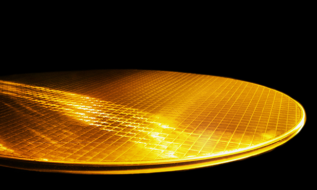
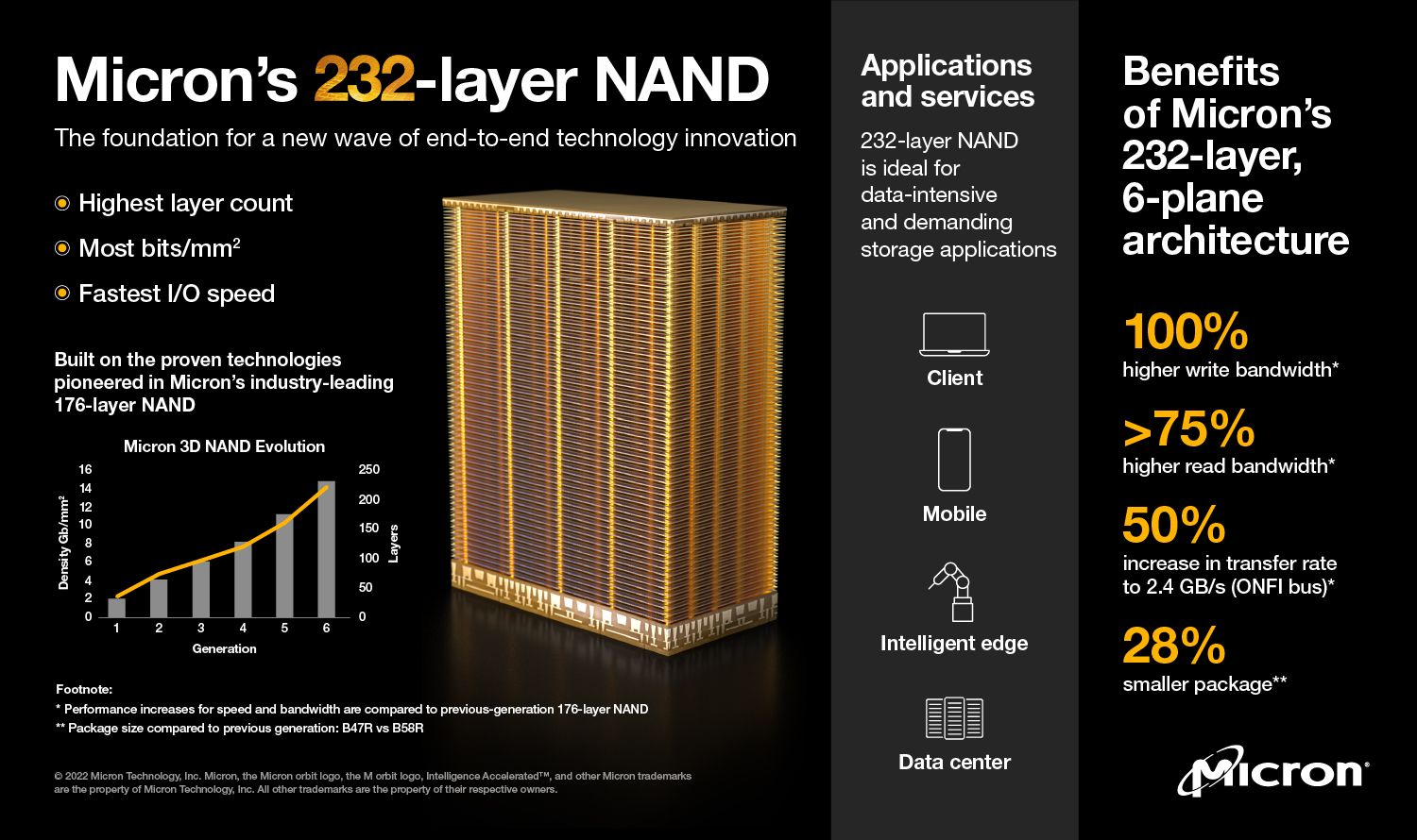
Forward of subsequent week’s Flash Reminiscence Summit, Micron this morning is asserting that their next-generation 232 layer NAND has begun delivery. The sixth era of Micron’s 3D NAND expertise, 232L is slated to supply each improved bandwidth and bigger die sizes – most notably, introducing Micron’s first 1Tbit TLC NAND dies, which at this level are the densest within the business. In keeping with the corporate, the brand new NAND is already delivery to clients and in Essential SSD merchandise in restricted volumes, with additional quantity ramping to happen later within the yr.
Micron first introduced their 232L NAND again in Might throughout their Investor Day occasion, revealing that the NAND could be obtainable this yr, and that the corporate meant to ramp up manufacturing by the top of the yr. And whereas that yield ramp remains to be ongoing, Micron’s Singapore fab is already able to producing sufficient of the brand new NAND that Micron is comfy in asserting it’s delivery, albeit clearly in restricted portions.
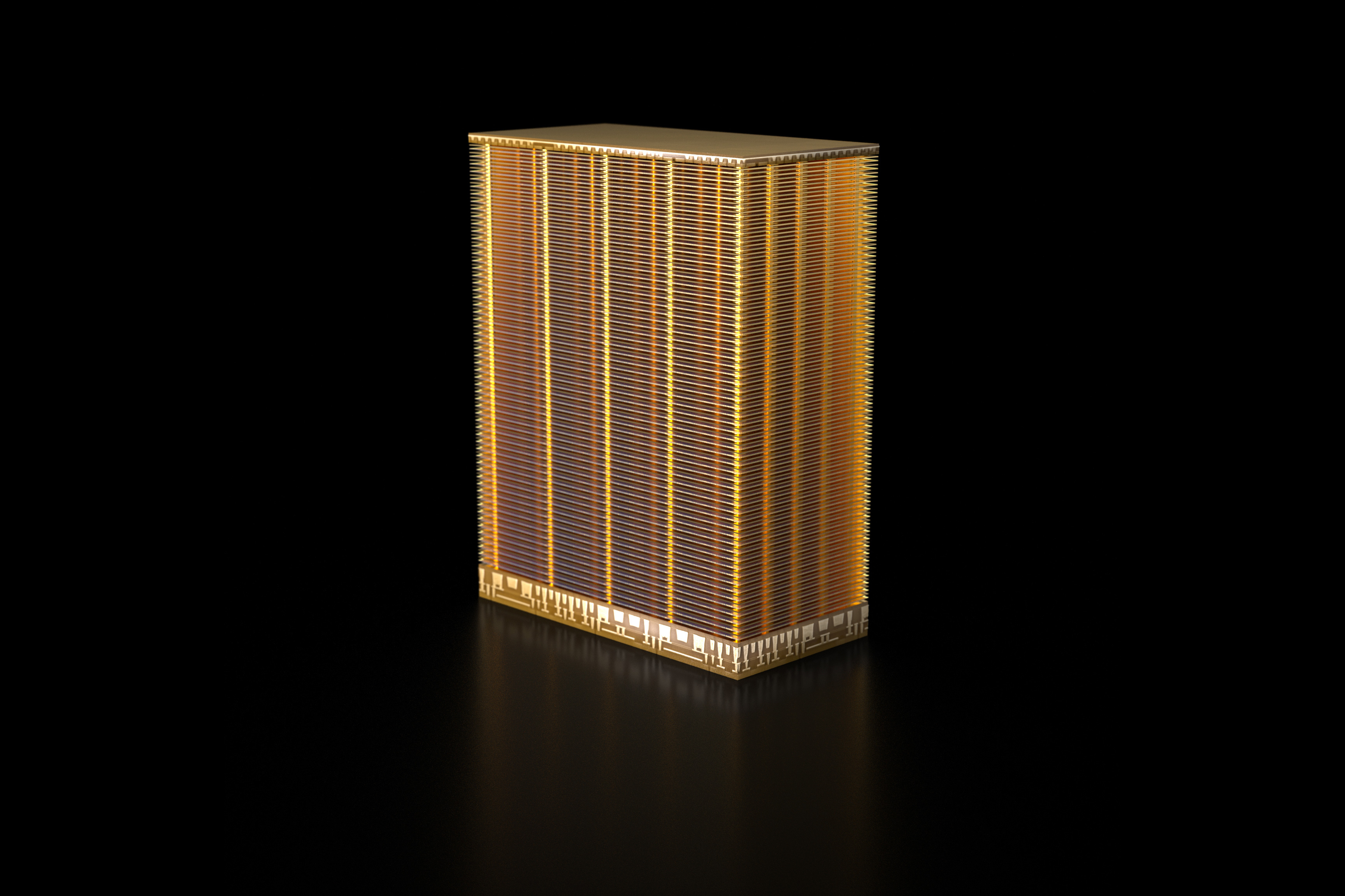
From a technical perspective, Micron’s 232L NAND additional builds upon the fundamental design components Micron honed in that era. So we’re as soon as once more a string stacked design, with Micron utilizing a pair of 116 layer decks, up from 88 layers within the earlier era. 116 layer decks, in flip, are notable as that is the primary time Micron has been in a position to produce a single deck over 100 layers, a feat beforehand restricted to Samsung. This in flip has allowed Micron to provide cutting-edge NAND with simply two decks, one thing that might not be doable for for much longer as firms push towards designs with over 300 complete layers.
Micron’s NAND decks proceed to be constructed with their charge-trap, CMOS underneath Array (CuA) structure, which sees the majority of the NAND’s logic positioned underneath the NAND reminiscence cells. Micron has lengthy cited this as giving them an ongoing benefit in NAND density, and that’s as soon as once more on present for his or her 232L NAND. In keeping with the corporate they’ve achieved a density of 14.6 Gbit/mm2, which is about 43% denser than their 176L NAND. And, in keeping with Micron, wherever between 35% to 100% denser than competing TLC merchandise.
| Micron 3D TLC NAND Flash Reminiscence | ||
| 232L (B58R) |
176L (B47R) |
|
| Layers | 232 | 176 |
| Decks | 2 (x116) | 2 (x88) |
| Die Capability | 1 Tbit | 512 Gbit |
| Die Dimension (mm2) | ~70.1mm2 | ~49.8mm2 |
| Density (Gbit/mm2) | 14.6 | 10.3 |
| I/O Velocity | 2.4 MT/s (ONFi 5.0) |
1.6 MT/s (ONFI 4.2) |
| Program Throughput | ? | ? |
| Planes | 6 | 4 |
| CuA / PuC | Sure | Sure |
The improved density has allowed Micron to lastly produce their first 1Tbit TLC die, which from a productization standpoint signifies that Micron can now additionally produce 2TB chip packages by stacking 16 of their 232L dies. That is excellent news for SSD capacities, which on the high-end are sometimes restricted by the variety of packages that may be positioned. Although it does imply that there’s a possible lack of efficiency at decrease capacities because of a lower parallelism from implementing fewer packages.
On the identical time, Micron has additionally been engaged on the scale of their chip packaging, and because of this whereas the bigger capability signifies that their die dimension has elevated on a generational foundation (we estimate ~70.1mm2 given Micron’s density figures), they’ve nonetheless shrunk their chip packaging by 28%. In consequence, a single chip package deal is down from 12mm x 18mm (216mm2) to 11.5mm x 13.5mm (~155mm2). So for Micron’s downstream clients, the mix of the larger capability and bodily smaller packages for Micron’s NAND signifies that machine producers can minimize down on the quantity of area they allocate to NAND packages, or go the opposite route and attempt to cram in much more packages into an identical quantity of area.
In addition to density enhancements, the newest era of Micron’s NAND can be permitting the corporate to improve their {hardware} to reap the benefits of newer I/O applied sciences, in addition to to implement their very own enhancements to extend switch speeds. The large information right here is that Micron has elevated the variety of planes inside their NAND die from 4 to six, additional enhancing the parallelism obtainable inside every die. Quad (4) airplane designs grew to become frequent within the earlier era of NAND, and because the density of NAND grows, so too are the variety of planes to ensure that switch charges to maintain up with these larger densities. Micron has confirmed that the planes in 232L NAND provide impartial reads, although they aren’t being fairly as specific on what sort of wordline dependencies stay for writes.
This improve in parallelism, together with improved inside switch charges, has allowed Micron to considerably enhance their per-die learn and write speeds. In keeping with the corporate, learn speeds have improved by over 75% over their 176L era NAND, and in the meantime write speeds have outright doubled.
Coupled with this, Micron has additionally applied the newest era of ONFi on their peripheral logic. Finalized in 2021 and now rolling out within the first NAND merchandise, ONFi will increase controller-NAND switch charges by 50%, bringing it to 2400MT/second. ONFi 5.0 additionally launched a brand new NV-LPDDR4 signaling technique, which is accessible with the identical 2400MT/s charge however, because it’s primarily based on LPDDR expertise, consumes much less energy. In keeping with Micron, they’re seeing per-bit vitality switch financial savings of over 30%, which makes for a big discount in vitality consumption. Although as at all times with these kinds of comparisons, it’s value noting that the bandwidth good points exceed the vitality financial savings (50% vs. 30%), so our expectation is that general vitality consumption goes to go up for high-performance merchandise that run on the quickest speeds supported by Micron’s 232L NAND.
As for productization, Micron is pitching 232L NAND as a full stack alternative for 176L NAND – which means that Micron considers it appropriate for all the things from cell and IoT to purchasers and information middle merchandise. To that finish, the corporate is already making preliminary shipments to their clients, together with their very own Essential subsidiary. As with previous generations of Micron NAND, beginning early with Essential permits the corporate to get some hands-on expertise in creating full-featured merchandise with their new NAND earlier than they roll it into their very own enterprise tools. Apparently, nonetheless, Micron isn’t asserting any new Essential merchandise proper now, which strongly implies that Essential goes to start implementing the brand new NAND in present merchandise. If that’s the case, then Essential clients will need to take note of what’s happening and what revision of a drive they’re shopping for, because the bigger 1Tb die might have efficiency implications for merchandise initially designed round 512Gbit dies.
Wrapping issues up, at the moment’s announcement must be the tip of the iceberg for Micron’s 232L shipments. With quantity ramping anticipated to proceed by way of this finish of this calendar yr, Micron’s plans name for the corporate to considerably improve the quantity of next-generation NAND they’re delivery, going properly past these preliminary volumes. In the end, which means merchandise outfitted with 232L NAND are going to be comparatively sparse for this yr, and can decide up in 2023 following the amount ramp. So whereas Micron’s 232L NAND is certainly delivery, from a client standpoint we’re doubtless nonetheless a number of months off (or extra) from seeing it turning into a standard fixture in SSDs and different merchandise.
