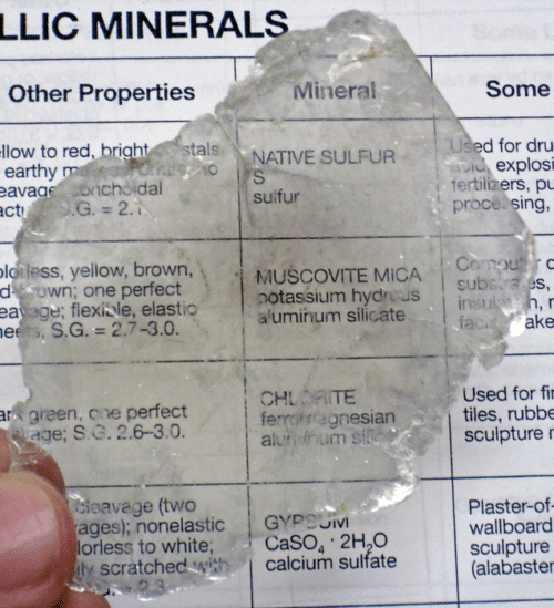
Many two-dimensional supplies with distinct electrical and bodily traits are being thought-about for the following era of digital gadgets. One such materials is muscovite mica (MuM).
MuM has drawn curiosity as an ultra-flat substrate for creating versatile electrical gadgets, much like how graphene has. Nonetheless, MuM is an insulator, not like graphene. It’s composed of layers of silicon (Si), aluminium (Al), and potassium (Ok), but it surely’s electrical properties are unclear. Significantly, it’s unclear how the traits of MuMs with single and few molecule layer thicknesses work. This is because of a quantum phenomenon often known as “tunnelling.” Due to this, it has been difficult to understand the conductivity of skinny MuM.
Professor Muralidhar Miryala from Shibaura Institute of Know-how (SIT), Japan, Professors M. S. Ramachandra Rao, Ananth Krishnan, and Mr. Ankit Arora, a PhD scholar, from Indian Institute of Know-how Madras, India, have just lately noticed a semiconducting behaviour in skinny MuM flakes, characterised by {an electrical} conductivity that’s 1000 occasions higher than that of thick MuM.
With a view to forestall tunnelling, the researchers stored the contact electrodes aside by 1 m whereas exfoliating skinny MuM flakes of various thickness onto silicon (SiO2/Si) substrates. Once they measured {the electrical} conductivity, they found that because the flakes have been lowered to fewer layers, the change to a conducting state occurred steadily. They found that for MuM flakes smaller than 20 nm, the present various with thickness, rising by an element of 1000 for a ten nm thick MuM (5 layers thick), versus a 20 nm thick MuM.
The “hopping conduction mannequin” proposes that the noticed conductance is brought on by a rise within the conduction band provider density with the discount in thickness. Merely mentioned, when MuM flakes turn into thinner, much less vitality is required to switch electrons from the strong bulk to the floor. This makes it less complicated for electrons to enter the “conduction band,” the place they might journey round freely and conduct electrical energy. The explanation for the rise in provider density was attributed by the researchers to the impacts of Ok+ ion-contributed floor doping (impurity addition) and MuM crystal construction leisure.
This discovery is important as a result of it reveals that the band construction of skinny exfoliated sheets of MuM is corresponding to that of vast bandgap semiconductors. This makes skinny MuM flakes an ideal materials for two-dimensional digital gadgets which can be each versatile and strong, along with its distinctive chemical stability. “MuM is understood for its distinctive stability in harsh environments comparable to these characterised by excessive temperatures, pressures, and electrical stress. The semiconductor-like habits noticed in our examine signifies that MuM has the potential to pave the best way for the event of strong electronics,” says Prof. Miryala.
Entry their analysis right here.
