A brand new technique for creating 3D built-in circuit connections has now been developed. It really works at low temperatures and doesn’t require exterior strain.
A brand new approach for the direct three-dimensional bonding of copper electrodes with silver was created by researchers from Osaka College’s Versatile 3D-System Integration Laboratory. This method can decrease the worth and vitality wants of latest digital merchandise. The event of extra energy-efficient and compact next-generation sensible devices may benefit from the work carried out right here.
Digital units are utilizing three-dimensional built-in circuits increasingly more incessantly. These topologies can preserve house and reduce the quantity of fabric wanted to attach the wires as in comparison with conventional 2D circuits. Opposite to the established know-how used for typical built-in circuits, dependable 3D connections require novel strategies. “Our course of could be carried out beneath light situations, at comparatively low temperatures and with out added strain, however the bonds have been in a position to face up to over one thousand cycles of thermal surprising from -55 to 125 ºC,” first creator Zheng Zhang says.
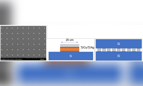
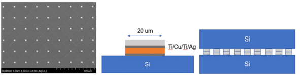
The 2 copper surfaces that might be joined utilizing this novel approach are first sputtered with silver at room temperature. The silver layers have been then heated to anneal them, which triggered “stress migration,” a microscopic alteration within the floor. An appropriate efficient space between the 2 silver layers was ensured by the floor roughening brought on by the stress launch throughout annealing. Consequently, even at a comparatively low annealing temperature, bonding could also be carried out with out the appliance of strain. In ten minutes, everlasting connections as small as 20 micrometres could possibly be created. Moreover, this process solely wants reasonable temperatures (180 °C) and will function in an environment.
Utilizing photographs from scanning electron microscopy and atomic pressure microscopy, the group was in a position to affirm the floor roughness of the sputtered and annealed chips. “This know-how is anticipated to contribute to chips with a excessive density of interconnects and superior 3D packaging,” senior creator Katsuaki Suganuma says.
